Design and Modelling of Tunnel Field Effect Transistor- using TCAD Modeling
Article Sidebar
Main Article Content
Abstract
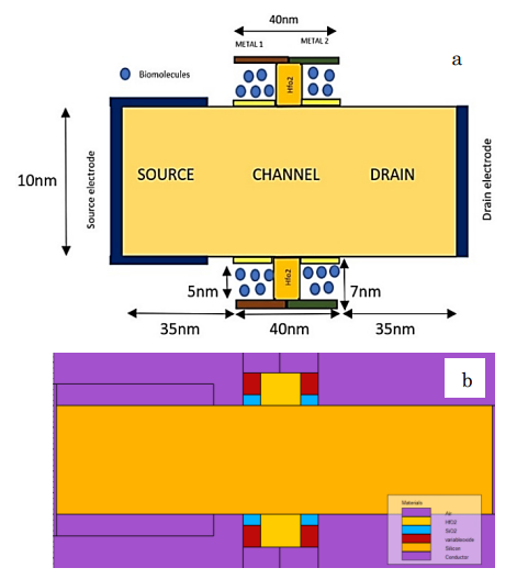
The purpose of this research was to suggest a junction-less strategy for a vertical Tunnel Field Effect Transistor, which would increase the device's efficiency. In this study, we examine the similarities and differences between a negative capacitor TFET and a vertically generated TFET with a source pocket and a heterostructure-based nanowire gate. And how the channel transit impacts the output qualities of a sub-100 nanometer sized device. The Silvaco TCAD (a commercially available tool) was used to simulate a tri-layer high-K dielectric made of hafnium zirconium oxide (HZO) and titanium dioxide (TiO2) materials as gate stacking to the V-TFET and GAA-NC-TFET structures, and the tunnelling and transport parameters were calibrated experimentally. A short bandgap material, GaSb, in the home region to enhance carrier tunnelling via the mentioned three source (GaSb)-channel (Si) heterojunction at varying biases were utilized. Motion, tube length, and saturating velocity are only few of the transport channel characteristics that are investigated. As a result of the building's vertical orientation, the electric field is enhanced, allowing for an ION current of up to 104 Am2. The most unexpected result of this device is that a high ION/IOFF may increase mobility and reduce saturation velocity, perhaps reducing the drain voltage at saturation. The proposed biosensor's sensitivity was multiplied by 108 when vertical and lateral tunnelling were used in tandem. We apply a variety of optimisation strategies to deal with this problem, despite the fact that quantum confinement reduces the effect of mobility variations on device performance. When biomolecules were positively charged, the drain current increased, and when they were negatively charged, the drain current decreased.
Article Details
References
Q. Huang et al., “First foundry platform of complementary Tunnel-FETs in CMOS baseline technology for ultralow-power IoT applications: Manufacturability, variability and technology roadmap,” in Int.Electron Devices Meeting (IEDM) Tech. Dig., Washington, DC, USA,2015, pp. 1–4.
Y.-H. Guan, Z.-C. Li, D.-X. Luo, Q.-Z. Meng, and Y.-F. Zhang, “Characteristics of cylindrical surrounding-gate GaAsxSb1?x/InyGa1?yAs heterojunction tunneling field-effect transistors,” Chin. Phys. B, vol. 25, no. 10, Aug. 2016, Art. No. 108502.
H. W. Kim and D. Kwon, “Steep switching characteristics of L-shaped tunnel FET with doping engineering,” IEEE J. Electron Devices Soc., vol. 9, pp. 359–364, 2021.
L. F. Pinotti, F. H. Cioldina, A. R. Vaza, L. C. J. Espíndolaa, and J. A. Diniza, “Vertical MOS and tunnel FETs in the same silicon pillar structure with Al and TiN gate electrodes,” Microelectron. Eng., vol. 231, Jul. 2020, Art. no. 111399.
E. Memisevic et al., “Individual defects in InAs/InGaAsSb/GaSb nanowire tunnel field-effect transistors operating below 60 mV/decade,” Nano Lett., vol. 17, no. 7, pp. 4373–4380, jun. 2017.
V. K. Chinni et al., “V-shaped InAs/Al0.5Ga0.5Sb vertical tunnel FET on GaAs (001) substrate with ION = 433?A/?m at VDS = 0.5V,” IEEE J. Electron Devices Soc., vol. 5, pp. 53–58, 2017.
T. Rosca, A. Saeidi, E. Memisevic, L.-E. Wernersson, and A. M. Ionescu, “An experimental study of heterostructure tunnel FET nanowire arrays: Digital and analog figures of merit from 300K to 10K,” in Int. Electron Devices Meeting (IEDM) Tech. Dig., San Francisco, CA, USA, 2018, pp. 1–4.
R. H. Dennard, F. H. Gaensslen, V. L. Rideout, E. Bassous, and A. R. LeBlanc, ‘‘Design of ion implanted MOSFET’s with very small physical dimensions,’’ IEEE J. Solid-State Circuits, vol. SSC-9, no. 5, pp. 256–268, Oct. 1974.
G. A. Brown, P. M. Zeitzoff, G. Bersuker, and H. R. Huff, ‘‘Scaling CMOS: Materials & devices,’’ Mater. Today, vol. 1, no. 7, pp. 20–25, 2004, doi: 10.1016/S1369-7021(04)00051-3.
G. E. Moore, Cramming More Components onto Integrated Circuits. New York, NY, USA: McGraw-Hill, 1965.
U. Dutta, M. K. Soni, and M. Pattanaik, ‘‘Design & optimization of gateall-around tunnel FET for low power applications,’’ Int. J. Eng. Technol., vol. 7, no. 4, pp. 2263–2270, 2018.
Q. Zhang, W. Zhao, and A. Seabaugh, ‘‘Low-subthreshold-swing tunnel transistors,’’ IEEE Electron Device Lett., vol. 27, no. 4, pp. 297–300, Apr. 2006.
J. Appenzeller, Y. M. Lin, J. Knoch, and P. Avouris, ‘Band-to-band tunneling in carbon nanotube field-effect transistors,’ Phys. Rev. Lett., vol. 93, no. 19, Nov. 2004, Art. no. 196805.
R. Gandhi, Z. Chen, N. Singh, K. Banerjee, and S. Lee, ‘‘Vertical Si-nanowire n-type tunneling FETs with low sub-threshold swing (50 mV/decade) at room temperature,’’ IEEE Electron Device Lett., vol. 32, no. 4, pp. 437–439, Feb. 2011.
V. Saripalli, A. Mishra, S. Datta, and V. Narayanan, ‘‘An energy-efficient heterogeneous CMP based on hybrid TFET-CMOS cores,’’ in Proc. 48th Design Automat. Conf. (DAC), 2011, pp. 729–734.
M. Ionescu and H. Riel, ‘‘Tunnel field-effect transistors as energy efficient electronic switches,’’ Nature, vol. 479, pp. 329– 337, May 2011.
K. Boucart and A. M. Ionescu, ‘‘Double-gate tunnel FET with high-K gate dielectric,’’ IEEE Trans. Electron Devices, vol. 54, pp. 1725–1733, Jul. 2007.
M. U. Sohag, M. S. Islam, K. Hosen, M. A. I. Fahim, M. M.H. Sarkar, and J. Park, ‘‘Dual source negative capacitance GaSb/InGaAsSb/InAs heterostructure based vertical TFET with steep subthreshold swing and high on-off current ratio,’’ Results Phys., vol. 29, Oct. 2021, Art. no. 104796, doi: 10.1016/j.rinp. 2021.104796.
Saeidi et al., ‘‘Near hysteresis-free negative capacitance InGaAs tunnel FETs with enhanced digital and analog figures of merit below VDD=400 mV,’’ in IEDM Tech. Dig., Dec. 2018, pp. 13.4.1–13.4.4, doi: 10.1109/IEDM.2018.8614583.
Goel, S. Rewari, S. Verma, S.S. Deswal, R.S. Gupta, IEEE Sensor. J. 21 No 15, 16731 (2021).
N. Paras, S.S. Chauhan, International Conference on Advances in Computing and Communication Engineering (ICACCE-2019).
W.C. Ma, IEEE T. Electron Dev. 64 No 3, 1390 (2017).
A. Goel, S. Rewari, S. Verma, R.S. Gupta, IEEE Electron Devices Kolkata Conference (EDKCON-2018).
Y. Lu, G. Zhou, L. Rui, L. Qingmin, Q. Zhang, T. Vasen, S.D. Chae, IEEE Electron Dev. Lett. 33 No 5, 655 (2012).
M. Abdullah-Al-Kaiser, D.J. Paul, Q.D.M. Khosru, IEEE Region 10 Humanitarian Technology Conference (R10-HTC-2017).
L. Lin, C. Li, Z. Zhang, E. Alexov, J. Chem. Theory Comput. 9 No 4, 2126 (2013).